Purpose
The RT7249 is a current mode step-down converter with the input voltage range from 4.5V to 18V and provides 3A outputcurrent. This document explains the function and use of the RT7249 evaluation board (EVB), and provides information to enable operation, modification of the evaluation board and circuit to suit individual requirements.
Introduction
General Product Information
The RT7249 is a high efficiency, monolithic synchronous step-down DC/DC converter with a power switch.The buck converter can deliver up to 3A output current from 4.5V to 18V input supply. The RT7249’s current-mode architecture and external compensation allow the transient response to be optimized over a wide input range and loads. Cycle-by-cycle current limit provides protection against shorted output and soft-start eliminates input current surge during start-up. The RT7249 also provides under-voltage protection and thermal shutdown. PWM frequency is adjustable by the ROSC pin and Power Switch current limit can also be adjusted by the RLIM pin. The low current (<3µA) in shutdown mode provides output disconnection, enabling easy power management in bettery-powered systems. The RT7249 is available in the WQFN-16L 4x4 package.
Product Feature
-
Buck Regulator
►4.5V to 18V Input Voltage Range
►3A Output Current
►Internal N-Chanel MOSFETs
►Current Mode Control
►Adjustable PWM Frequency
►Adjustable Output from 0.8V to 15V
►Adjustable Soft-Start Time
►Stable with Ceramin Output Capactiors
►Cycle-by-Cycle Current Limit
►Input Under-Voltage Lockout
►Output Under-Voltage Protection
►Thermal Shutdown
-
Power Switch
►±15% Current-Limit Accuracy at 1.2A
►Adjustable Current Limit : 75mA to 2580mA
►Meet USB Current-Limiting Requirements
►Reverse Input-Output Voltage Protection
►Built Soft-Start
►120mΩ High-Side MOSFET
►Operating Range : 2.5V to 5.5V
Key Performance Summary Table
|
Key Features
|
Evaluation Board Number : PCB067_V1
|
|
Default Input Voltage
|
12V
|
|
Max Output Current
|
3A
|
|
Default Output Voltage
|
5V
|
|
Default Marking & Package Type
|
RT7249GQW, WQFN-16L 4x4
|
|
Operation Frequency
|
500kHz Switching Frequency
|
Bench Test Setup Conditions
Headers Description and Placement
Please carefully inspect the EVB IC and external components, comparing them to the following Bill of Materials, to ensure that all components are installed and undamaged. If any components are missing or damaged during transportation, please contact the distributor or send e-mail to evb_service@richtek.com.
Test Points
The EVB is provided with the test points and pin names listed in the table below.
|
Test point/
Pin name
|
Signal
|
Comment (expected waveforms or voltage levels on test points)
|
|
VIN
|
Input voltage
|
Power Input. Supply voltage range is from 4.5V to 18V. Must bypass with a suitable large ceramic capacitor.
|
|
PGND
|
Ground
|
Power Ground. The exposed pad must be soldered to a large PCB and connected to PGND for maximum thermal dissipation.
|
|
AGND
|
Ground
|
Analog Ground.
|
|
SS
|
Soft-Start
|
Soft-Start Time Setting. SS controls the soft-start period. Connect a capacitor from SS to GND to set the soft-start period. An internal current source (6μA) charges 0.1μF capacitor and sets the soft-start period to 13.5ms. If SS is floating, the SS charge current will decrease to 1/128μA and charge 30pF capacitor to set the soft-start period to 4ms.
|
|
COMP
|
Compensation Node
|
Compensation Node. COMP is used to compensate the regulation control loop.Connect a series RC network from COMP to GND. In some cases, an additional capacitor from COMP to GND is required.
|
|
ROSC
|
Frequency Setting
|
Switching Frequency Setting.
|
|
RLIM
|
Current Limit Setting
|
Current Limit Setting. Switch current limit threshold can be set by an external resistor. Current limit value is from 75mA to 2580mA. The value of 10kΩ ≤ RILIM ≤ 210kΩ is recommended.
|
|
EN_SW
|
Enable Power Switch test pin
|
Enable Control Input for Power Switch.
|
|
FAULT
|
FAULT test point
|
Active-Low Open-Drain Output. Asserted during over current, over
temperature, or reverse voltage conditions.
|
|
SW_OUT
|
Power Switch Output
|
Power Switch Output.
|
|
SW_IN
|
Power Switch Input
|
Power Switch Input. Supply voltage range is from 2.5V to 5.5V.
|
|
FB
|
Feedback Voltage
|
Feedback Voltage Input. This pin is connected to the converter output. It is used to set the output of the converter to regulate the desired value via an resistive divider.
|
|
LX
|
Switch Node test pin
|
Switch Node. Output of the internal high-side MOSFET. Connect this pin to external low-side N-MOSFET, inductor and bootstrap capacitor.
|
|
BOOT
|
BOOT Node test pin
|
Bootstrap Supply for High-Side Gate Driver. Connect a 1μF ceramic
capacitor between the BOOT and LX pins.
|
|
V5V
|
V5V test pin
|
BG Driver Bias Supply. Decouple with a 1μF X5R/X7R ceramic capacitor between the V5V and GND pins.
|
|
EN
|
Enable test pin
|
Enable Control Input for Buck Converter. A logic-high enables the converter; a logic-low forces the device into shutdown mode.
|
Power-up & Measurement Procedure
1. Set the jumper at JP1 to connect terminals 1 and 2, connecting Vout to SW_IN
2. Apply a 12V nominal input power supply to the VIN and GND terminals.
3. Connect an external load up to 6A to the VOUT and GND terminals and verify the output voltage and current.
Output Voltage Setting
Set the output voltage with the resistive divider (R1, R2) between External Input and GND with the midpoint connected to VREFIN. The output is set by the following formula :

Schematic, Bill of Materials & Board Layout
EVB Schematic Diagram
Bill of Materials
|
Reference
|
Qty
|
Part Number
|
Description
|
Package
|
Manufacture
|
|
C1, C2, C10
|
3
|
UMK325BJ106MM
|
10µF/X5R/50V/1206
|
C-1206
|
TAIYO YUDEN
|
|
C3, C7, C9
|
3
|
C1608X7R1H104KT000N
|
0.1µF/X7R/50V/0603
|
C-0603
|
TDK
|
|
C4, C5, C8
|
3
|
C3225X5R1E226MT
|
22µF/X5R/25V/1210
|
C-1210
|
TDK
|
|
C6
|
1
|
|
NC/1210
|
|
|
|
C11, C16
|
2
|
0603B472K500
|
4.7nF/X7R/50V/0603
|
C-0603
|
WALSIN
|
|
C12, C19
|
2
|
|
NC/0603
|
|
|
|
C14, C15
|
2
|
C1608X5R1E105KT000E
|
1µF/X5R/25V/0603
|
C-0603
|
TDK
|
|
C17
|
1
|
|
NC
|
|
|
|
C18, C20
|
2
|
C1608X7R1H104KT000N
|
0.1µF/X7R/50V/0603
|
C-0603
|
TDK
|
|
C3_1
|
1
|
|
NC
|
|
|
|
GP1
|
1
|
|
EN
|
|
|
|
GP3, GP4, GP8
|
3
|
|
GND
|
|
|
|
GP5
|
1
|
|
Vin
|
|
|
|
GP6
|
1
|
|
Vout
|
|
|
|
GP7
|
1
|
|
SW_OUT
|
|
|
|
GP9
|
1
|
|
SW_IN_S
|
|
|
|
GP10
|
1
|
|
SS
|
|
|
|
GP14
|
1
|
|
SW
|
|
|
|
GP15
|
1
|
|
V5V
|
|
|
|
GP16
|
1
|
|
nFAULT
|
|
|
|
GP17
|
1
|
|
BOOT
|
|
|
|
GP11
|
1
|
|
RSOC
|
|
|
|
GP12
|
1
|
|
RLIM
|
|
|
|
GP13
|
1
|
|
ENSW
|
|
|
|
JP1
|
1
|
|
SW_IN
|
|
|
|
J1
|
1
|
|
Vin, GND
|
|
|
|
L2
|
1
|
NR8040T4R7N
|
4.7µH
|
|
TAIYO YUDEN
|
|
R1
|
1
|
0603 40K2 1%
|
40.2k/0603
|
R-0603
|
|
|
R2
|
1
|
|
7.68k/0603
|
R-0603
|
|
|
R3
|
1
|
|
20k/0603
|
R-0603
|
|
|
R4
|
1
|
|
53.6k/0603
|
R-0603
|
|
|
R5
|
1
|
|
10k/0603
|
R-0603
|
|
|
R6, R7, R8
|
3
|
|
100k/0603
|
R-0603
|
|
|
U1
|
1
|
RT7249GQW
|
DC/DC Converter
|
WQFN-16L 4x4
|
RICHTEK
|
|
Z1, Z2, Z3, Z4
|
4
|
|
SIP-1P-M
|
|
|
|
Z11, Z12, Z13, Z14
|
4
|
|
FK_1
|
|
|
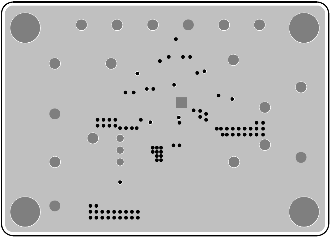
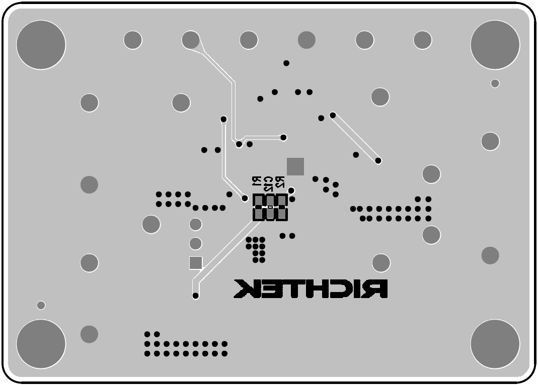
PCB Layout
Top View (1st layer)
PCB Layout—Inner Side (2nd Layer)
PCB Layout—Inner Side (3rd Layer)
Bottom View (4th Layer)